Hybrid FinFET-Silicon Photonics Technology for Ultra-low Power Optical I/O
Imec has demonstrated ultra-low power, high bandwidth optical transceivers through hybrid integration of silicon photonics and FinFET CMOS technologies.
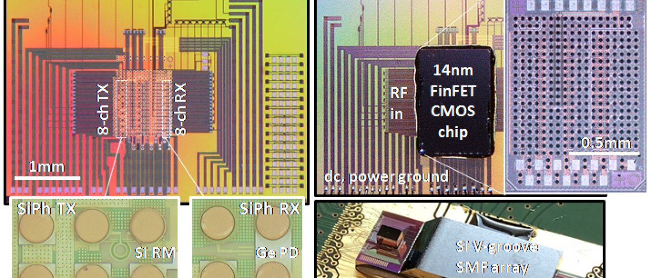
In the presented work, a differential FinFET driver was co-designed with a silicon photonics ring modulator, achieving a 40Gb/s NRZ optical modulation at 154fJ/bit dynamic power consumption. The receiver included a FinFET trans-impedance amplifier (TIA) optimized for operation with a Ge wave guide photo diode, enabling 40Gb/s NRZ photo detection with an estimated sensitivity of -10dBm at 75fJ/bit power consumption. High-quality data transmission and reception was also demonstrated in a loop-back experiment at 1330nm wavelength over standard single mode fiber (SMF) with 2dB link margin. Finally, a 4x40Gb/s, 0.1mm2 wavelength-division multiplexing (WDM) transmitter with integrated thermal control was demonstrated, enabling bandwidth scaling beyond 100Gb/s per fiber.
“The demonstrated hybrid FinFET-silicon photonics platform integrates high-performance 14nm FinFET CMOS circuits with imec’s 300mm silicon photonics technology through dense, low-capacitance Cu micro-bumps. Careful co-design in this combined platform has enabled us to demonstrate 40Gb/s NRZ optical transceivers with extremely low power consumption and high bandwidth density,” says Joris Van Campenhout, director of the Optical I/O R&D program at imec.
This work has been carried out as part of imec’s industrial affiliation R&D program on Optical I/O and was presented at the 2018 Symposia on VLSI Technology and Circuits (June 2018) in a “late news” paper. Source: Imec
You can definitely see your skills within the article you write.
The world hopes for more passionate writers such as you who are not afraid to mention how
they believe. All the time go after your heart.