3D Printing Shortens PCB Prototyping Cycle
Among manufacturers, there is a common understanding that the more complex the concept, the longer it takes to produce a market-ready functional object. This is especially relevant for the highly competitive electronics industry, where product complexity is continuously increasing and improved time-to-market is a primary business objective.
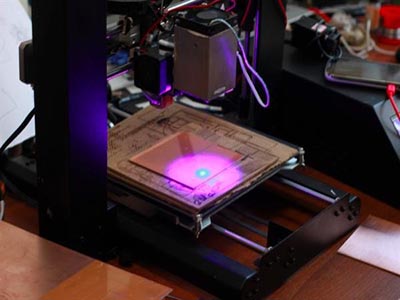
It all begins with the Printed Circuit Board (PCB) and electronics design and development companies’ need for shorter, faster and more efficient product development cycles. Most of today’s PCB prototypes are produced by traditional subtractive manufacturing methods, often by overseas vendors—most often located in Asia. Producing the PCB is a boring multistage process, including milling, drilling, film transfer, and plating machines; copper etching baths; and a press. Standard turnaround times are generally two to three weeks, although circuit prototypes can often be produced in less time for a substantial urgency fee.
An even greater challenge is when design complexity rises, as in the creation of professional multi layer prototype boards needed to create innovative new applications and electronic products. A tiny mistake in design, resulting in a poor circuit, could lead to risky product recalls and other quality problems.
To avoid costly mistakes of this kind, there is usually a need for proof-of-concept, design validations, and other interim steps on the way to a final full-board prototype. This means that even after the PCB prototype has been produced and tested, problems are often discovered and designs need to be updated, further increasing the lead time and cost for each PCB, making frequentative design and testing virtually impossible.